

INDIAN ARMED FORCES CHIEFS ON
OUR RELENTLESS AND FOCUSED PUBLISHING EFFORTS

SP Guide Publications puts forth a well compiled articulation of issues, pursuits and accomplishments of the Indian Army, over the years

I am confident that SP Guide Publications would continue to inform, inspire and influence.

My compliments to SP Guide Publications for informative and credible reportage on contemporary aerospace issues over the past six decades.
- Admiral Dinesh K. Tripathi assumes Command of the Indian Navy as 26th Chief of the Naval Staff
- Prime Minister witnesses 'Bharat Shakti' – a Tri-Services Firing and Manoeuvre Exercise in Pokhran, Rajasthan
- Interim Defence Budget 2024-25 — An Analysis
- Union Defence budget 2024
- Prime Minister Modi Commemorates Indian Navy Day in a Grand Ceremony
- Prime Minister Modi Flies in the LCA Tejas
- New Chapter in India-Italy Defence Ties
- Airpower beyond Boundaries
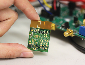
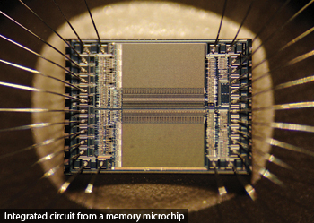
The precious chip
Our engineering colleges need to give much more focus on practical rather than theoretical knowledge, without which our already late chip manufacturing will not get the required impetus, since we actually need to leapfrog capacity building in this sphere
What is usually referred to as chip, IC or microchip or a semiconductor is an integrated circuit or monolithic electrical circuit of a generally solid chemical element or compound (usually Silicon) that can conduct electricity under some conditions making it a good medium for control of electric current, the conductance depending on the voltage applied to the control electrode or on the intensity of the irradiation by visible light, IR, UV or X-rays. The specific properties of a semiconductor depend on the impurities added to it.
The name ‘chip’ came because the set of electronic circuits on one small plate (chip) of semiconductor material. Chips can be very compact, having up to several billion ‘transistors’ and other electronic components in an area the size of a thumbnail, with further compression possible as technology advances – in range of tens of nanometers. The performance of chips is quite high because their small size allows short traces, which in turn allows low power logic, like CMOS, to be used at fast switching speeds. Digital memory chips and application specific integrated circuits (ASIC) are examples of the chip family that are important to the modern information society. The cost of designing and developing a complex chip is quite high but when spread across typically millions of production units the individual chip cost is minimised.
In terms of applications, the chip has become the foundation of modern electronics. They are being used in manufacturing computers, space research, medical sciences and the like. A transistor is one of the most widely used chip, available in multiple kinds which can be used in diverse fields like for manufacturing logic gates as basis of the design of digital circuits. Transistors are also used in analog circuits as switches to respond to a constant range of inputs with a uninterrupted range of outputs since common analog circuits include amplifiers and oscillators.
Other chip applications are in the form of circuits or mixed-signal circuits, latter acting like the translator between digital circuits and analog circuits. Additionally there are ‘power chips’ consisting of devices which have integrated circuits. Power chips are used in those applications which require very high current or voltage requirements. Semiconductors devices application which involves combination of power semiconductor technology and Integrated Technology (IC) are called smart power devices. The main use of such devices is in the field of space research.
Finally, is the use of semiconductor devices in making high speed computer parts, calculators, telephones, medical equipment etc in addition to being extensively used in robotics. Research is ongoing to find new avenues and areas where the applications of chips can help gain better results in terms of performance and other parameters. In current research projects, integrated circuits are also developed for sensory applications in medical implants and other bio-electronic devices.
According to the report by Global Industry Analysts, Inc. released in December 2013 on Semiconductor Fabrication Material markets, global market for Semiconductor Fabrication Material is projected to reach $33.3 billion by 2018, driven by steady increase in IC fabrication activity in response to growing demand for electronic devices. Growing demand for electronic chip fabrication as a result of increasing production of mobile computing devices (notebooks, smart-phones, tablet PCs) is benefiting growth in the semiconductor fabrication material market.
While consumer electronics and appliances remain the primary driver of growth, emerging applications in automotive electronics, medical device electronics, defence and aerospace electronics, including state-of-the-art weaponry, are poised to fuel future growth in the market. The shift towards miniaturisation is also driving growth in the market by requiring specialisation of back-end fabrication. In the coming years, the persistent financial challenges and the pressure on capital will continue to mark the distinct evolution of pure-play foundries and fabless suppliers. The fabless model of microchip production will continue to gain prominence, given its unrivaled cost benefits. To say that the lack of indigenous chip manufacture in India was a strategic void would be an understatement especially with Japan being the largest chip manufacturer in the region and even China having 95 fabs way back in 1995 compared to none in India.
The Indian semiconductor sector comprises pre-fabrication, fabrication and post-fabrication verticals. Despite the current slowdown in global markets, the Indian semiconductor market has shown sustained growth over the years. In 2007, the Indian Semiconductor Association (ISA)-Frost and Sullivan estimated the Indian semiconductor market to be worth $4.56 billion, which had already risen to $7.59 billion by year 2010. Gartner had estimated India’s semiconductor consumption reached $8 billion in 2012 (7.4 per cent increase from 2011) and that this consumption would reach $9.6 billion in 2013 (20 per cent increase over 2012).
After decades of wait, the Government of India has finally accorded “in principle” approval on February 14, 2014, for setting up of two Semiconductor Wafer Fabrication (FAB) manufacturing facilities in the country. These fabs would enhance the information and economic security of India, give boost to the Electronics System Design and Manufacturing (ESDM) ecosystem in the country and will provide defence offset obligations for electronic procurement through ESDM products. The two consortiums that stand approved to set up thr fab facilities are: one, Jaiprakash Associates along with IBM (USA) ans Tower Jazz (Israel) with an outlay of about Rs. 26,300 crore for a fab at Greater Noida producing 30,000 wafer of 300 mm size in the beginning, technology nodes approved being 90, 65 and 45 nano meter (nm) in Phase I and 28 nm in Phase II, with the option of establishing a 22 nm in Phase III; and, two, Hindustan Semiconductor Manufacturing Corporation (HSMC) along with Microelectronics (France/Italy) and Silterra (Malaysia) for a fab in Gujarat with an outlay of about Rs. 25,250 crore of 40,000 wafer starts per 300 mm size, technology nodes proposed being 90, 65 and 45 nm nodes in Phase I and 45, 28 and 22nm nodes in Phase II.
 While on one hand India has the gigantic burden of 4.53 crore unemployed (mostly youth), on the other, we also are churning out some 9,60,000 engineer graduates every year; large number of high quality with advanced English skills that fit well with the requirements of the knowledge-intensive semiconductor industry. Growth of the Indian semiconductor design market is expected to lead to an increase in the number of engineers employed by this segment. Already job advertisements from multiple companies (there are about 150 semiconductor design companies in Bengaluru alone) are spread across the web seeking qualified persons in semiconductor VLSI design, software and embedded design, chemical and material science engineering, electrical and control systems engineering and the like. Here, the euphoria needs to be tempered with the fact that in India we have the problem of hands on experience plus exposure to the product and end application with the first two fabs just about beginning to set up.
Product conceptualisation, management and analog design skills need to be advanced. To this end, our engineering colleges need to give much more focus on practical rather than theoretical knowledge, without which our already late chip manufacturing will not get the required impetus, since we actually need to leapfrog capacity building in this sphere. For this, our engineering colleges could tie up with industry players and co-locate labs with them to impart requisite practical training.
The government and the industry on the other hand should examine introduction of an institutionalised system of internships to provide the right engineer material in the required numbers to progress the chip industry. Even more important is the need to aim for the ultimate – totally indigenous chip design and development in place of foreign collaboration, which would be essential for our future weapon systems. This needs to be taken up on priority.
SP's MAI - CURRENT ISSUE